Track Down Those Memory Bugs!
Leo J. Scanlon
Inverness, FL
Problems with memory cells in your computer's RAM (where you do your programming) can sometimes be quite subtle. It would be clear that you had a bad cell somewhere if your computer responded to your question, ? FRE(1) by saying that you had 320 bytes free before you'd even put a program in. But what about the less obvious memory problems? A cell might only go strange when the cell next to it contains a five. Or it might work fine, but fail after a certain amount of time passes. Such subtle failures, fortunately relatively rare, can have you looking in vain for a bug in your program. Mr. Scanlon presents a sophisticated memory testing program here (in machine language, for any computer which uses the 6502 chip, Apple, CBM/PET, Atari, OSI, VIC). This program can uncover some of those more subtle cell failures.
If you just went out and bought a new tape recorder, a pair of jeans, or a quart of milk, you'd find out in short order just how good or bad the product is. If the tape recorder makes a Sousa march sound like a funeral dirge, back to the store it goes. Likewise, the jeans will show their quality after the first washing, and your nose knows if the milk is bad!
Unfortunately, faults in a computer memory board may not be that evident. Certainly, you will spot obvious defects – a crack in the board, missing chips, and the like – but if the board is operating at all, you'll probably need a diagnostic program to pinpoint any specific problem. This article presents one such program. It was developed on a Rockwell AIM 65 microcomputer, but it can run on any 6502-based computer, provided you alter the output routines. The general principles can, of course, be applied to other types as well.
Besides "dead" chips, which cannot store any data, memory boards have a variety of other potential problems. For example, some chips contain one or more bits that will not accept information, or bits that just hold the information briefly, then lose it. Other chips will not accept certain bit patterns, or affect other memory chips in the array. We can't hope to write a single program that will identify all possible errors, but the program given here will isolate most errors – or at least give you enough information to delve deeper into the problem.
The Test Algorithm
The diagnostic program in this article uses an algorithm that was implemented for 68000-based systems by Robert D. Grappel ("M68000 Diagnostic Program Tests Memory," EDN, April 15, 1981, pp. 157-158). This algorithm has two main loops. The first loop fills the tested portion of memory with increasing bit patterns; 000000002 is written into the first byte, 000000012 is written into the second byte, and so on. With this done, the second loop checks the memory contents and prints an error message each time a mismatch is detected.
The test then repeats, each time incrementing the contents of each byte. Thus, after 256 cycles, each byte has held all possible values. Note that the test is destructive; any pre-test information in the affected RAM will be eradicated.
The program described here also allows you to check for either hard failures or soft failures. Hard failures are those that cause the loss of ability to change the state of one or more bits, whereas soft failures allow a change, but revert back to the original state after a period of time. For soft failure testing, the time delay between write and read/verify has been set at one minute, arbitrarily.
Program Flowcharts
With the two tasks now defined, we can look at a program that will do the job. Before doing so, however, it will be helpful to investigate the overall structure of the two loops, by looking at their flowcharts.
Figure 1 shows the sequence of operations for the write loop, the loop that fills the test portion of memory with increasing bit patterns. This loop is preceded by some necessary initialization. First, the cycle count is set to 255. We actually want 256 cycles, but with a microprocessor that has only eight-bit registers (and memory locations), it is convenient to use 255, and plan ending the test when the cycle count has decremented past zero, to an all-ones (hex FF) state.
Next, the start pattern – the pattern that will be written into the first test location – is initialized to zero. Admittedly, zero is arbitrary. Since we will cycle through memory 256 times, each location will eventually receive every possible bit pattern. Therefore, it really doesn't matter which value goes into the first byte.
The microprocessor then calculates the byte count, by taking the difference between the specified end address and start address, and adding one. This is followed by a call to a set-up subroutine, which sets the "base address" equal to the starting address, fetches the start pattern and sets a byte index equal to zero. (The use of the terms base address and index here show that we plan to use one of the 6502's indexed addressing modes. These modes calculate an effective address by adding the contents of an index register – X or Y – to an absolute or indirect base address.)
Figure 1: Initialization and Write Sequences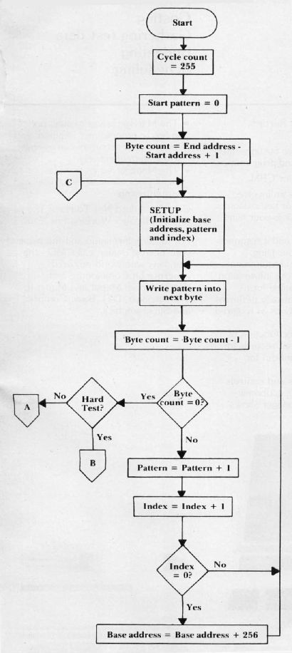
At this point, the microprocessor enters the actual write loop. It starts by writing a pattern into memory, decrementing the byte count, then checking whether test memory has been entirely filled with test patterns (byte count = 0). When the byte count is zero, the microprocessor branches to the read/ verify loop, at either its soft error test or hard error test entry point; path A or path B, respectively. Otherwise, pattern and index are incremented, in preparation for writing to the next byte.
When the index has been incremented past hex FF, and reaches zero, a new base address is calculated, by adding 256 to the existing base address. Again, this is necessary because our index registers are only eight bits wide. A nonzero index causes the microprocessor to loop back to write the next pattern into memory. This concludes our discussion of the write loop.
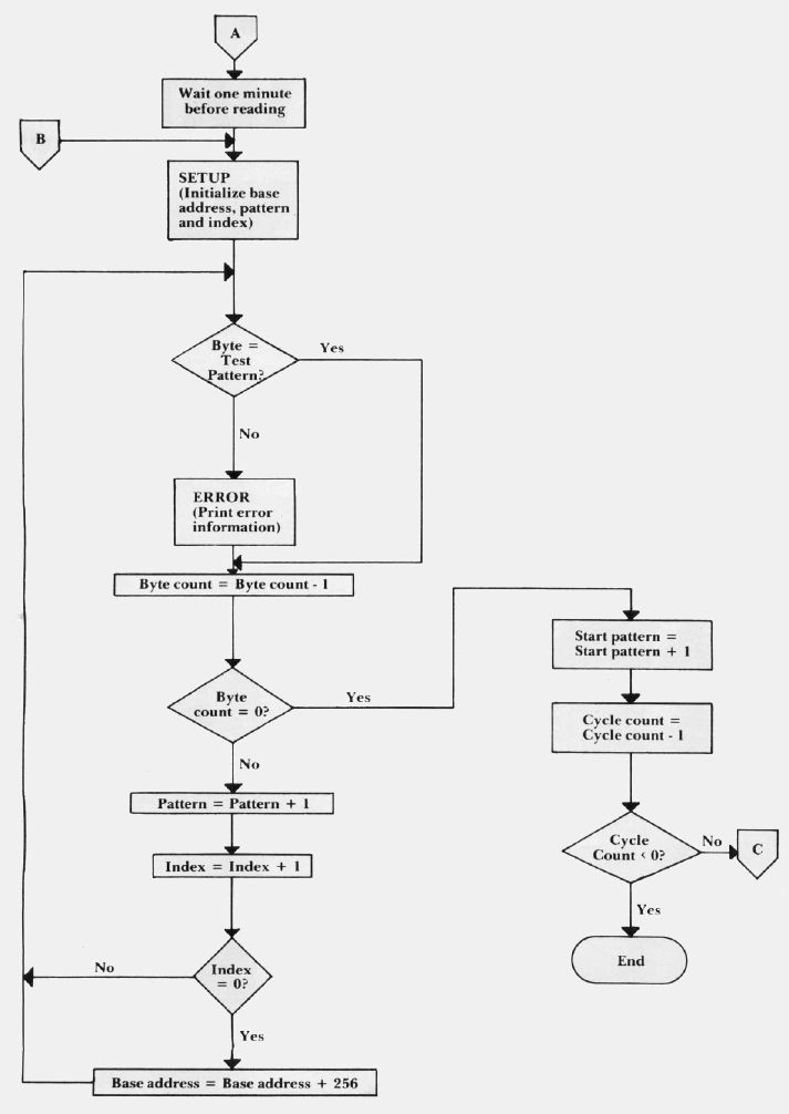
As expected, the sequence of the read/verify loop (Figure 2) is very similar to that of the write loop. However, the read/verify loop has two separate entry points, one for soft error testing (in which the loop is preceded by a one-minute time delay), and the other for hard error testing. The read/ verify loop begins with a call to the SETUP subroutine, to fetch the starting test pattern and reinitialize the base address and index.
With this initialization completed, the byte-by-byte comparisons begin. This consists of comparing the contents of each memory location against the test pattern that was written into it. If a mismatch is detected, the microprocessor calls an error subroutine, to print out the pertinent information – bad address, expected pattern and the pattern read. The rest of the read/verify loop is identical to the bottom of the write loop, except that when all locations have been read, the read/verify loop increments the start pattern and checks for end-of-test (cycle count less than zero). If further testing is necessary, the microprocessor branches back to the beginning of the write loop.
The Diagnostic Program
Now that you understand the criteria of the program and its sequences, we can look at the program itself. Program 1 shows the initialization and write sequence, the portion of the program that was flowcharted in Figure 1. Note that before executing the program, three parameters must be stored in zero page:
- Store the starting address in locations 00 and 01, with the low byte in 00.
- Store the ending address in locations 02 and 03, with the low byte in 02.
- Select soft error testing or hard error testing by storing a value of 00 or 01, respectively, in location 04.
Besides these five locations, the program uses 11 other zero page locations, as working storage. These include three parameters that have already been discussed–byte count (BCOUNT), starting address (STARTP) and base address (BADDR)–and four additional parameters which have yet to be discussed. Of these four, the working byte count (WCOUNT) is a byte count that gets decremented during each cycle. In fact, WCOUNT gets decremented twice during each cycle–once during a cycle through the write loop, then (after being reloaded with the byte count, BCOUNT) once again during the subsequent cycle through the read/verify loop.
The parameter SPAT is a save location for the test pattern. During the read/verify and write loops, the test pattern is held into the accumulator; SPAT saves the pattern while the accumulator is being used for other operations. The last two parameters, PADDR and ROTLOC, are used to hold information that gets printed out if an error occurs. Specifically, PADDR holds the effective address of the error location and ROTLOC holds the "should be" pattern and the "is" pattern (i.e., the expected pattern and the actual pattern).
Next come equates that reference three subroutines in the AIM 65 monitor: NUMA prints the contents of the accumulator, as two ASCII characters; OUTPRI sends one character to the print buffer; CRLOW initializes the display and printer to their "start" positions.
Program 1: Source Code for Initialization and Write Sequences
HDE ASSEMBLER REV 2.2
LINE#   ADDR    OBJECT  LABEL   SOURCE
01-0010 2000            ;THIS PROGRAM TESTS MEMORY FOR BOTH HARD AND
01-0020 2000            ;SOFT ERRORS.
01-0030 2000            ;BEFORE EXECUTING, STORE THE FOLLOWING
01-0040 2000            ;PARAMETERS IN MEMORY:
01-0050 2000            ;LOCS. 00 AND 01 = STARTING ADDRESS
01-0060 2000            ;LOCS. 02 AND 03 = ENDING ADDRESS
01-0070 2000            ;LOC. 04 = HARD ERROR (01) OR SOFT ERROR (00)
01-0080 2000            ;THE PROGRAM RETURNS TO THE MONITOR WHEN DONE.
01-0100 2000            ;USER-SUPPLIED PARAMETERS
01-0120 2000                    *=0
01-0130 0000            START   *=*+2               ; STARTING ADDR
01-0140 2000            END     *=*+2               ; ENDING ADDR
01-0150 2000            HARD    *=*+1               ; HARD/SOFT ERROR TEST SELECT
01-0170 0005            ; EQUATES FOR WORKING STORAGE IN ZERO PAGE
01-0190 0005            BCOUNT  *=*+2               ; BYTE COUNT
01-0200 0007            WCOUNT  *=*+2               ; WORKING BYTE COUNT
01-0210 0009            START   *=*+1               ; STARTING PATTERN
01-0220 000A            BADDR   *=*+2               ; BASE ADDRESS
01-0230 000C            SPAT    *=*+2               ; PATTERN IS SAVED HERE
01-0240 000D            PADDR   *=*+2               ; ERROR BYTE ADDRESS
01-0250 000F            ROTLOC  *=*+1               ; WORKING BYTE FOR PRINT ROUTINE
01-0270 0010            ; AIM 65 MONITOR SUBROUTINES
01-0290 0010            NUMA =$EA46                 ; PRINT A, AS TWO ASCII CHARS.
01-0300 0010            OUTPRI =$F000               ; OUTPUT A TO PRINT BUFFER
01-0310 0010            CRLOW =$EA13                ; RESET DISPLAY & PRINTER
01-0330 0010            ; INITIALIZATION SEQUENCE
01-0350 0010                    *=$200
01-0360 0200 A2 FF      INIT LDX #255                ; CYCLE COUNT = 255
01-0370 0202 A9 00      LDA #0                       ; STARTING PATTERN = 0
01-0380 0204 85 09      STA STARTP
01-0390 0206 38         SEC                          ; BYTE COUNT = END ADDR. -
01-0400 0207 A5 02      LDA END ; START ADDR. + 1
01-0410 0209 E5 00      SBC START
01-0420 020B 85 05      STA BCOUNT
01-0430 020D A5 03      LDA END+1
01-0440 020F E5 01      SBC START+1
01-0450 0211 85 06      STA BCOUNT+1
01-0460 0213 E6 05      INC BCOUNT
01-0470 0215 D0 02      BNE MLOOP
01-0480 0217 E6 06      INC BCOUNT +1
01-0490 0219 20 BC 02   MLOOP JSR SETUP                ; INITIALIZE COUNT, ADDR, INDEX
01-0510 021C            ;WRITE SEQUENCE
01-0530 021C 91 OA      WRITE STA (BADDR), Y           ; WRITE PATTERN INTO NEXT BYTE
01-0540 021E 85 OC      STA SPAT                       ;AND SAVE PATTERN
01-0550 0220 0220 38    SEC                            ; DECREMENT BYTE COUNT
01-0560 0221 A5 07      LDA WCOUNT
01-0570 0223 E9 01      SBC #1
01-0580 0225 85 07      STA WCOUNT
01-0590 0227 A5 08      LDA WCOUNT+1
01-0600 0229 E9 00      SBC #0
01-0610 022B 85 08      STA WCOUNT+1
01-0620 022D D0 0A      BNE INCP                       ; BYTE COUNT = 0?
01-0630 022F C5 07      CMP WCOUNT
01-0640 0231 D0 06      BNE INCP
01-0650 0233 C5 04      CMP HARD                       ; YES. GO READ/VERIFY
01-0660 0235 D0 23      BNE READH
01-0670 0237 F0 0C      BEQ READSLINE#   ADDR OBJECT  LABEL      SOURCE
01-0680 0239 A5 0C    INCP      LDA SPAT        ; NO. GET PATTERN
01-0690 023B 18                 CLC             ; AND INCREMENT IT
01-0700 023C 69 01              ADC #1
01-0710 023E C8                 INY             ; INCREMENT INDEX
01-0720 023F D0 DB              BNE WRITE       ; INDEX = 0?
01-0730 0241 E6 0B              INC BADDR+1     ; YES. ADD 256 TO BASE ADDRESS
01-0740 0243 D0 D7              BNE WRITE       ; AND GO WRITE TO NEXT BYTE
The rest of Program 1 shows the source code for the initialization sequence and the write loop. The programming is straightforward, so you should have no problem following it if you studied the flowchart in Figure 1. Note that the write loop is terminated when the byte count has been decremented to zero. At that time, we interrogate the contents of the user-specified parameter HARD (location $04), and branch to the read/verify sequence, at either READS (if HARD contains zero) or READH (if HARD contains a nonzero value).
The read/verify sequence, shown in Program 2, also follows its earlier flowchart (Figure 2), and needs no additional description. However, you may be interested in the one-minute time delay routine that gets executed if you are testing for soft errors. This routine, DELAY 1, generates the one-minute delay by executing a 300-millisecond delay routine (D300) 200 times! Readers who are interested in the details of this and other delay routines are referred to my book 6502 Software Design (Howard W. Sams & Co., 1980). Because the D300 uses the X Register – which holds our program's cycle count – the contents of that register must be saved on the stack while the time delay is being generated.
Program 2: Source Code for Read/Verify Sequence
LINE#   ADDR    OBJECT  LABEL SOURCE
01-0760 0245            ; READ/VERIFY SEQUENCE. ENTER HERE FOR SOFT
01-0770 0245            ; ERROR TESTING
01-0790 0245 8A         READS   TXA              ; SAVE X (CYCLE COUNT) ON STACK
01-0800 0246 48                 PHA
01-0810 0247            ; WAIT ONE MINUTE BEFORE BEGINNING TO READ
01-0820 0247 A9 C8      DELAY1  LDA #200         ; EXECUTION COUNT = 200
01-0830 0249 A2 A5      D300    LDX #$A5         ; LOAD X AND Y FOR A 300 MS. DELAY
01-0840 024B A0 EA              LDY #$EA
01-0850 024D CA         WAIT    DEX
01-0860 024E DO FD              BNE WAIT         ; LOOP UNTIL X = 0
01-0870 0250 88                 DEY
01-0880 0251 DO FA              BNE WAIT         ; LOOP UNTIL X = 0
01-0890 0253 38                 SEC              ; DECREMENT TIMING BYTE
01-0900 0254 E9 01              SBC #1
01-0910 0256 DO F1              BNE D300         ; LOOP UNTIL A = 0
01-0920 0258 68                 PLA
01-0930 0259 AA                 TAX              ; RESTORE CYCLE COUNT
01-0940 025A            ; ENTER HERE  FOR HARD ERROR TESTING
01-0950 025A 20 8C 02   READH   JSR SETUP       ; REINITIALIZE PARAMETERS
01-0960 025D DD1 0A     COMP    CMP (BADDR), Y  ; BYTE = TEST PATTERN?
01-0970 025F 85 OC              STA SPAT
01-0980 0261 F0 03              BEQ DECBC
01-0990 0263 20 A1 02           JSR ERROR       ; NO. PRINT ERROR MESSAGE
01-1000 0266 38         DECBC   SEC             ; YES. DECREMENT BYTE COUNT
01-1010 0267 A5 07              LDA WCOUNT
01-1020 0269 E9 01              SBC #1
01-1030 026B 85 07              STA WCOUNT+1
01-1040 026D A5 08              LDA WCOUNT+1
01-1050 026F E9 00              SBC #0
01-1060 0271 85 08              STA WCOUNT+1
01-1070 0273 D0 04              BNE INCP1       ; BYTE COUNT = 0?
01-1080 0275 C5 07              CMP WCOUNT
01-1090 0277 F0 0B              BEQ DECCC
01-1100 0279 A5 0C      INCP1   LDA SPAT        ; NO. GET PATTERN
01-1110 027B 69 01              ADC #1          ; AND INCREMENT IT
01-1120 027D C8                 INY             ; INCREMENT INDEX, TOO
01-1130 027E DO DD              BNE COMP        ; INDEX = 0?
01-1140 0280 E6 0B              INC BADDR+1     ; YES. ADD 256 TO BASE ADDRESS
01-1150 0282 D0 D9              BNE COMP        ; AND GO COMPARE NEXT BYTE
01-1160 0284 E6 09      DECCC   INC STARTP      ; INCREMENT START PATTERN
01-1170 0286 CA                 DEX             ; DECREMENT CYCLE COUNT
01-1180 0287 E0 FF              CPX #$FF        ; COUNT CYCLE NEGATIVE?
01-1190 0289 D0 8E              BNE MLOOP
01-1200 028B 00                 BRK             ; YES. RETURN TO MONITOR
The final program, Program 3, shows the source code for the set-up subroutine (SETUP), followed by the error printout subroutine (ERROR). As was mentioned previously, if the read/verify sequence reads a pattern that does not match the expected pattern, the error subroutine prints out three items of information: the address of the offending location, the expected pattern (the "S/B" pattern) and the pattern that is actually read (the "IS" pattern). As an aid to identifying faulty bits within a memory location, the S/B and IS patterns are printed in a binary representation. To do this, ERROR calls a second subroutine (BINARY) that left-rotates the contents of a working zero-page location, ROTLOC, eight times. After each rotate operation, BINARY outputs an ASCII 1 or ASCII 0 to the printer.
Figure 3 shows the kind of listing that the ERROR subroutine produces. To generate this listing on my AIM 65, I selected three locations within the monitor ROM – LOCATIONS $E000, $E001, and $E002 – knowing that a read/verify test on ROM will always fail. As you can see, the printout has been retyped for publication, because the AIM 65 printer output does not reproduce very well.
Program 3: Source Code for Set-Up and Error Subroutines
LINE#   ADDR    OBJECT  LABEL   SOURCE          PAGE 0004
01-1230 028C
01-1250 028C            ; THIS SUBROUTINE TRANSFERS THE BYTE COUNT TO
01-1260 028C            ; THE WORKING BYTE COUNT, SETS BASE ADDR =
01-1260 028c            ; START ADDR, FETCHES THE PATTERN, AND SETS INDEX = 0
01-1290 028C A5 05      SETUP   LDA BCOUNT      ; INITIALIZE WORKING BYTE COUNT
01-1300 028E 85 07              STA WCOUNT
01-1310 0290 A5 06              LDA BCOUNT+1
01-1320 0292 85 08              STA WCOUNT+1
01-1330 0294 A5 00              LDA START       ; TO BEGIN, BASE ADDR = START ADDR
01-1340 0296 85 0A              STA BADDR
01-1350 0298 A5 01              LDA START+1
01-1360 029A 85 0B              STA BADDR+1
01-1370 029C A5 09              LDA STARTP      ; INITIALIZE PATTERN
01-1380 029E A0 00              LDY #0          ; INDEX = 0
01-1390 02A0 60                 RTS
01-1410 02A1            ; PRINT ERROR INFORMATION
01-1420 02A1            ;  BAD ADDRESS (HEX)
01-1430 02A1            ;  S/B PATTERN (BINARY)
01-1440 02A1            ;  IS PATTERN (BINARY)
01-1460 02A1 98         ERROR   TYA             ; SAVE Y ON STACK
01-1470 02A2 48                 PHA
01-1480 02A3 18                 CLC             ; CALCULATE PRINT ADDRESS
01-1490 02A4 65 0A              ADC BADDR
01-1500 02A6 85 0D              STA PADDR
01-1510 02A8 A9 00              LDA #0
01-1520 02AA 65 0B              ADC BADDR+1
01-1530 02AC 85 0E              STA PADDR+1
01-1540 02AE 20 13 EA           JSR CRLOW       ; RESET DISPLAY AND PRINTER
01-1550 02B1 A0 00              LDY #0          ; PRINT LOC LINE
01-1560 02B3 B9 0B 03   LOOP1   LDA LINE1,Y
01-1570 02B6 20 00 F0           JSR OUTPRI
01-1580 02B9 C8                 INY
01-1590 02BA C0 07              CPY #7
01-1600 02BC D0 F5              BNE LOOP1
01-1610 02BE A5 0E              LDA PADDR+1
01-1620 02C0 20 46 EA           JSR NUMA
01-1630 02C3 A5 0D              LDA PADDRLINE#   ADDR    OBJECT          LABEL   SOURCE
01-1640 02C5    20 46 EA                JSR NUMA
01-1650 02C8    20 13 EA                JSR CRLOW
01-1660 02CB    B9 0B 03        LOOP2   LDA LINE1, Y   ; PRINT S/B LINE
01-1670 02CE    20 00 F0                JSR OUTPRI
01-1680 02D1    C8                      INY
01-1690 02D2    C0 0F                   CPY #15
01-1700 02D4    D0 F5                   BNE LOOP 2
01-1710 02D6    A5 OC                   LDA SPAT
01-1720 02D8    20 F6 02                JSR BINARY
01-1730 02DB    20 13 EA                JSR CRLOW
01-1740 02DE    AO 0F                   LDY #LINE3-LINE1
01-1750 02E0    B9 0B 03        LOOP3   LDA LINE1, Y    ; PRINT IS LINE
01-1760 02E3    20 00 F0                JSR OUTPRI
01-1770 02E6    C8                      INY
01-1780 02E7    C0 17                   CPY #23
01-1790 02E9    D0 F5                   BNE LOOP3
01-1800 02EB    68                      PLA
01-1810 02EC    48                      PHA
01-1820 02ED    A8                      TAY
01-1830 02EE    B1 0A                   LDA (BADDR), Y
01-1840 02F0    20 F6 02                JSR BINARY
01-1850 02F3    68                      PLA
01-1860 02F4    A8                      TAY
01-1870 02F5    60                      RTS
01-1890 02F6                    ;PRINT PATTERN IN BINARY FORMAT
01-1910 02F6    A0 08                   BINARY LDY #8
01-1920 02F8    85 0F                   STA ROTLOC
01-1930 02FA    26 0F           ROTATE  ROL ROTLOC       ;IS BIT A 1 OR A 0?
01-1940 02FC    90 04                   BCC SBZERO
01-1950 02FE    A9 31                   LDA #'1'         ; IT'S A 1?
01-1960 0300    D0 02                   BNE PBIT
01-1970 0302    A9 30           SBZERO  LDA #'O'         ;IT'S A 0
01-1980 0304    20 00 F0        PBIT    JSR OUTPRI
01-1990 0307    88                      DEY
01-2000 0308    D0 F0                   BNE ROTATE
01-2010 030A    60                      RTS
01-2030 030B                    ;MESSAGES FOR ERROR SUBROUTINE
01-2050 030B    20 20           LINE1   .BYT ' LOC.='
01-2060 0312    20 20           LINE2   .BYT ' S/B='
01-2070 031A    20 20           LINE3   .BYT ' IS='
01-2080 0322                            .END
ERRORS = 0000      END OF ASSEMBLY = 0321
Execution Times For The Test Program
Having seen the source code listings, you now know that the test program occupies slightly more than a page of memory; to be exact, it occupies 290 bytes. However, you're probably more curious about how long the program takes to execute – which translates to how long you will have to stand around before you know whether or not the memory is "bug-free."
In testing for hard errors, the program takes about 25 seconds to test 1024 (or 1 K) bytes, if your computer has a 1-MHz clock. This means that it will take six minutes and 45 seconds to test a 16K-byte board.
In testing for soft errors, the program introduces a one-minute time delay between each write and read/verify sequence. And since the program executes 256 cycles, soft error testing will always take two hours and 16 minutes more than hard error testing, regardless of how much memory is being tested! Therefore, it will take roughly two hours, 22 minutes and 45 seconds to test a 16K board for soft errors. Clearly, it's best to check for hard errors first, then re-check for soft errors if you're still having problems.
Figure 3: Sample Error Printout
LOC.= E000
S/B = 00000000
IS  = 01000110
LOC.= E001
S/B = 00000001
IS  = 01010010
LOC.= E002
S/B = 00000010
IS  = 01001111
LOC.= E000
S/B = 00000001
IS  = 01000110
LOC.= E001
S/B = 00000010
IS  = 01010010
LOC.= E002
S/B = 00000011
IS  = 01001111
LOC.= E000
S/B = 00000010
IS  = 01000110
LOC.= E001
S/B = 00000011
IS  = 01010010
LOC.= E002
S/B = 00000100
IS  = 01001111
    .
    .     (253 more sets of listings follow.)
    .