How To Use The 6560 Video Interface Chip
Dale Gilbert
Henegar, AL
The 6560 Video Interface Chip, the VIC chip, provides low cost, high resolution, color video to a color monitor or a color television, and it also incorporates a sound generator, A/D converters [analog/digital], and even a light pen feature.
The 6560, some RAM, a crystal, a few bus drivers, and a little decode logic is all the hardware that is required to add color and sound to a microprocessor that has an expansion bus.
The VIC capabilities include on-chip sync generation, screen grid size of up to 192 horizontal dots by 200 vertical dots, two character sizes, three independent programmable tone generators, a white noise generator, an amplitude modulator, screen centering, on-chip DMA address generation, and two modes of color operation.
The 6560 VIC is manufactured by MOS Technology, Inc.. Commodore Business Machines incorporates the 6560 in their VIC-20 Computer. I purchased my chip from Falk-Baker Associates, 382 Franklin Avenue, Nutley, New Jersey 07110, for $14.95.
6560 Software
To produce colored characters, VIC addresses two blocks of memory at the same time. This address method produces twelve bits of data. The eight bit block of memory is called the Character Pointer Block (called the screen memory on the VIC-20).
The second block of memory is called the Character Color Block (called the color nibble area on the VIC-20). This block contains four-bit character color data.
VIC takes the character pointer data, left shifts it three times, and adds the result to the character cell base address contained in bits zero through three of register five.
VIC then puts the result on the address bus which addresses another block of memory called the Character Cell Block (called character bit maps on the VIC-20). This block of memory is eight bits wide. The data obtained from this address is video information on an 8 × 8 character matrix. The matrix is eight bytes high and eight bits wide.
VIC takes the four-bit character color data and, if the MSB is 0, the character matrix will be displayed in high resolution mode. If the MSB is one, the character matrix will be displayed in the multicolor mode.
When the high resolution mode is selected and when bit-3 of register-F is a zero, all one bits of the character cell data will be displayed in the background color and all zero bits will be in the foreground color. The three remaining bits of the character color data specify the color of the foreground. The color of the background is specified by bits four through seven of register-F. If bit-3 of register-F is 1, the one bits of the character cell data will be displayed in foreground color and the zero bits will be displayed in background color.
If bit-3 of register-F is one, all the character cell matrix will have the same color background. If bit-3 is a zero, all the character cell matrix will have common character colors.
When the multicolor mode is selected (MSB of the character color data is one), there is a pairing of bits of the character cell data. The character matrix now is a 4 × 8 dot matrix with each dot's color determined by the code of each pair. The code has four possibilities: 00,01,10,11. If a dot code is 00, its color is the background color specified by bits four through seven of register-F. If the code is 01, the dot color is the same as the external border color specified by bits zero through two of register-F. If the code is ten, the dot color is the foreground color specified by the three bits of the character color data. If the code is 11, the color of the dot is specified by bits four through seven of register-E.
VIC produces a TV raster of up to twenty-two columns by up to twenty-three rows of character matrix surrounded by a border. The base address of the character pointer block contains the first upper left pointer for that character matrix. The base address plus one of the character pointer blocks contains the pointer for the next right character matrix. It is the responsibility of the MPU to manipulate the pointers in the character pointer block of memory. A whole raster of repeated characters (character matrix) can be obtained by just repeating the pointers in the character pointer block.
6560 Hardware
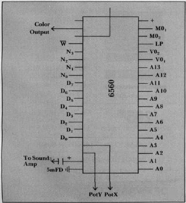
The 6560 VIC has fourteen address pins (A0-A13) and twelve data pins (D0 - D11). When the 02 clock is high, the MPU can place an address on the address pins and read or write data into any of the sixteen eight-bit registers via data pins D0 - D7. VIC decodes the address pins and selects registers zero through F when address 1000 through 100F (the VIC-20's VIC chip ignores the A 15 line) is placed on the address pins.
The address pins are input pins when 02 is one; if 02 is zero, then these pins are output address pins.
When the 02 clock is one, the MPU can also write or read data to the character pointer RAM, the character color RAM, and the character cell RAM. The character cell memory may be RAM, ROM, or both. The base address of the character cell block and/or the character pointer can be changed by modifying a register in the VIC.
When the 02 clock is low, the VIC addresses memory in such a way that the character pointer RAM and the character color RAM is selected at the same time. VIC must receive character pointer data on D0 through D7 and character color data on D8 through D11 at the same time.
The R/W pin four is an input only pin and must be driven by the MPU when 02 is one and held high when 01 is one.
Pins 38 and 39 are the master clock inputs. The 6560 VIC requires a 14.31818 MHz, two phase, five volt, non-overlapping signals. The master clock uses a standard 14.31818 MHz crystal (4× color) and the delay of 74LS gates to give a non-overlapping signal. Resistors R1 and R2 are used to give extra pull up to CMOS levels. CMOS gates don't seem fast enough for this clock.
Pins 35 and 36 are the system output clock used for system timing and driving the clock of the 6512 MPU (if used). A 6502 MPU can be used by feeding pin 36 to the 00 IN pin on the 6502. Removing the original 00 signal and wiring this new 00 is the only alteration needed on the mother MPU.
Because the 6502 address lines are active when 01 is 1, the expansion address lines to the VIC and its associated memory must be isolated from the MPU bus during this time.
The data bus should also be buffered and gated for this same reason.
The system clocks are five volt, non-overlapping, 1.02 MHz signals.
Pin 19 provides the sound output which must be fed to an amplifier to a drive speaker. The output impedence is approximately 1000 ohms.
Pin 3 is the output pin for the composite sync and the luminance signal. This pin is an open drain which makes it easy to shift to the needed voltage level for a RF modulator, TV first video amplifier, or a black and white CRT monitor.
In the following wiring diagram, diodes K3, K4, K5, and K6; resistors R5, R6, and R7; and C1 make up the level shifter for a TV output or video monitor output.
The VIC is a superior CRT controller for a B/W monitor due to the varying levels of luminance required for a color picture. VIC can produce varying shades of gray.
Pin 2 provides the composite color signal. This signal contains the color phase and amplitude information plus the 3.58MHz burst signal. Pin 2 is a high impedence output buffer which can be applied to the first chroma amplifier of a TV, color monitor, or RF modulator.
Pins 17 and 18 are the input pins for the Pot-X and Pot-Y analog to digital converters. A pot is used to charge an external capacitor tied to the pot wiper and fed to pin 17 or 18. These pins are systematically pulled to ground after each charge voltage reading. The voltage is digitized and deposited in register 8 or 9.
Pin 37 is the light gun/pen pin. The voltage of triggering is approximately 2.5 volts on the falling edge. Holding this pin low clears registers 6 and 7. The values of registers 6 and 7 represent the horizontal and vertical positions of the current dot being scanned. The light gun/pen option is only available on a 6560-101 which is sometimes identified by a white dot on the case of the IC.
Address decoding must be provided so that the character color nibble RAM will be selected, when the character pointer RAM is addressed by the VIC, but not selected when the MPU addresses the character pointer RAM. A data bus transceiver must be provided to isolate the nibble bus from the byte bus along with the logic for this transceiver. The logic must enable the MPU to read or write to the nibble bus when the 02 clock is one.
The expansion 02 may be used as the E(02) if the expansion 02 has no more than one LS gate delay and it is the true MPU 02. If these provisions can't be met, connect E(02) to the V02 (pin 36).
This author used addresses 1000 through 100F for the VIC; 2000 through 23FF for the character pointer block; 2400 through 27FF for the character color block; and 2800 through 2BFF for the character cell block.
The addition of a 6560, a few RAM chips, and a few gates will free up and complement many a MPU.
|
Color Code Auxiliary/Background/Border/Foreground 0 BLACK 1 WHITE 2 RED 3 CYAN 4 MAGENTA 5 GREEN 6 BLUE 7 YELLOW 8 ORANGE 9 LIGHT ORANGE A PINK B LIGHT CYAN C LIGHT MAGENTA D LIGHT GREEN E LIGHT BLUE F LIGHT YELLOW |
|
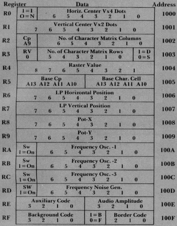
VIC Control Registers
Abbreviations: I = Interlace N = None Interlace CP = Character Pointer Base Address R = Raster V = Value S = 8 × 8 Matrix D = 16×8 Matrix B = Common Background F = Common Foreground LP = Light Pen Sw = Switch |
|
|