The Single-Board 6502
Eric Rehnke
EPROM SIMULATOR
Ever since I first saw an ad for the Pragmatic Design's 'Debug Memory' (DBM-1) board I became fascinated by the design concept of this rather unique RAM board.
Basically, the DBM-1 is a 2K×8 RAM board for the S-100 bus which can simulate a 2K ROM or EPROM (or 2-1K ROMS) to a target system.
In other words, the same 2K block of RAM that appears to the development system as normal random-access memory, appears to the target system as a 2K ROM/EPROM through a cable plugged into that ROM socket.
It can achieve this nature by viture of its dual-port RAM design. This means that the same memory can be accessed from two separate systems each with its own address and data bus.
The benefit of this type of arrangement becomes obvious when you consider that everything that is written to the 2K block of RAM in the development system also appears in the ROM/EPROM address space of the target system.
Now, instead of developing a program inside your large development system, then burning an EPROM, and installing it in the target system to see if it works, you simply write the program into the RAM on the “Debug Memory” board.
It will then appear in the target system and can be tested immediately. If there's a problem, no EPROM to erase and reprogram, simply write the corrected software to the DBM-1. The updated software automatically appears in the target system.
Saves lots of time!!!
The biggest benefit of the EPROM simulator will be gained when developing software for small, dedicated controllers which have no built-in monitor software of their own. But, using the simulator will also save lots of time when writing programs for semi-smart single-board computers like AIM or SYM, for example.
Another, not so obvious, use of the simulator is for developing a character generator for a video board. The video board can even be plugged into the development system itself.
(Most memory-mapped video boards also use this dual-port RAM concept in their design).
Of course, for the simulator to function most efficiently, the assembler in the development system must be able to assemble an object program to a location in memory other than specified by the program counter equate in the source code of that program. This is called 'assembling with offset'.
Say the EPROM socket in the target system resides at $F800-$FFFF in that system while the EPROM Simulator is addressed at $C000 in the development system. To be able to have a program assembled to run at $F800 while actually residing at $C000, it needs to be assembled with an offset. Get it?
My assembler (from HDE) has this capability so I decided to design my own EPROM Simulator. (I couldn't use the DBM-1 since it was designed for the S-100 bus).
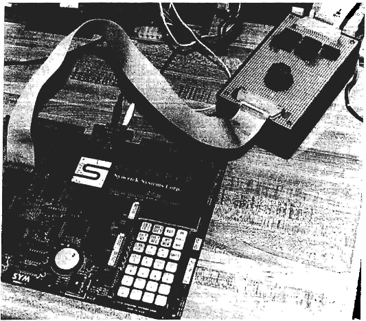
Also, my version is rather more simplified than the DBM-1 since there were some features I didn't feel I needed - like trap address comparators, daisy chaining, etc.
I built it on an HDE prototyping card and designed it to simulate the 2708, the TI 2716 or the Intel 2716. This should satisfy most of the requirements. Later, when 4K EPROMS get cheaper, I'll build a version to simulate them.
So far, I've used the simulator to speed up software development for my SYM system, look forward to using it with my AIM system, and will use it to develop a PET character generator for an upcoming video board design.
As I have found, the EPROM Simulator is a development tool which can really save time and improve the efficiency of the system designer.