PARALLEL BUS REVEALED
Concluding the four-part series that for the first time teaches advanced XL users how to build an I/O connector for the powerful, ultra-fast Parallel Bus Interface. This article includes an assembly language listing that requires MAC/65 or Atari Assembler Editor. You will also need access to an EPROM burner. The three earlier installments ran in the January, February and March 1985 issues of Antic.
Last month we looked at a design for a serial I/O device using a readily
available USART chip. This month we'll design address decoding logic for
the device and see how to add a status register and an interrupt register
to it. We'll also look at some example software for the device ROM. But
first, a little about last month's design.
This USART design is a simplest case design. Writing to any
address in the $D100-$D1FF range puts a character into the transmit buffer
and it will be sent out the serial I/O line. Reading any address in the
same range gets the last received character from the receive buffer.
The easiest way to test this arrangement is to tie the serial
input and output lines (USART pins 20 and 25) together. If you write a
character to the transmit buffer and wait a few milliseconds, you should
be able to read the same character from the receive buffer. All this assumes
that we're decoding addresses and that we have some software in ROM, so
let's get on with those details.
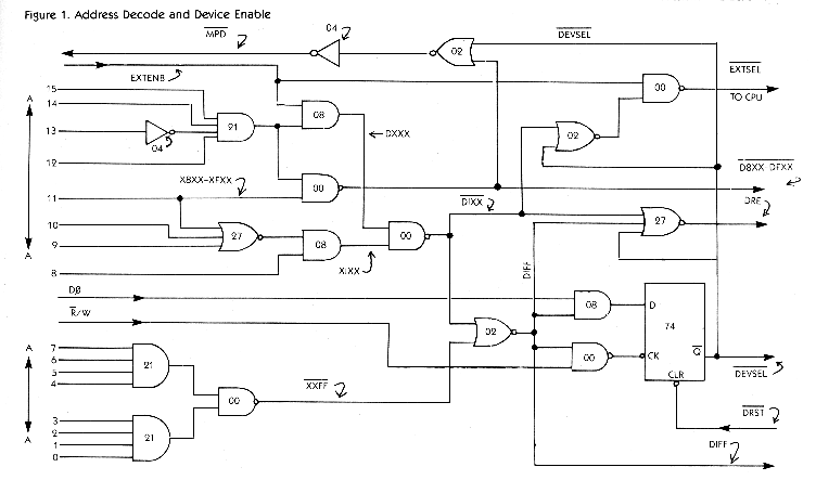
ADDRESS DECODER
Figure 1 is a schematic diagram of an address decoder to provide ROM
selection and device register selection.
The output signal $D8XX-$DFXX, combined with the Device Select
signal (DEVSEL), provides the Math Pack Disable signal (MPD) to disable
the floating point ROM in the CPU so it doesn't contend with our ROM for
the data bus. We can use the same signal to select our ROM. This allows
us to remove some of the logic from last month's circuit. Just remove the
wires from 1C4 pins 6, 5, 4,13,12 and 11 and connect MPD to ROM pin 20.
(See last month's Figure 2).
The signal $DlFF selects the Device Enable Latch. When a write
signal clocks the 74HCT74 latch, the value of the Data 0 line (D0) will
be stored. Writing 1 to address $DlFF selects our external device. Writing
0 deselects it. $DlFF can also be used later to select an interrupt register.
By combining it with DEVSEL and $DlXX, we get a Device Register
Enable signal (DRE). We'll use this signal instead of part of the logic
in last month's circuit to make the device registers work. Just remove
the wires from 1C4 pins 3,2 and 1, and connect DRST to 1C5 pin 13.
The CPU External Enable signal (EXTENB) lets our device know
the computer wants to talk to device registers (or RAM in a more complex
application). That signal is combined with DEVSEL and $DlXX to make an
External Select signal (EXTSEL) to turn off CPU RAM so as to avoid bus
contention.
DEVICE RESET
The Device Reset signal (DRST) comes from last month's circuit and
resets the device select latch any time the CPU generates a RESET signal.
You've probably noticed that this month's schematics are a little
different from last month's. Since last month's circuit is the basic recipe
for our device, we included IC location assignments and pin numbers.
This month's article deals with several options you might or
might not use, so we're giving you IC type numbers and no pin assignments
for general logic functions. The number inside or next to a symbol is its
type number. For example, 00 means 74HCT00.
Since all the logic is 74HCT series, we just need to use the
last digits of the type number to identify a part. Also, be aware that
we use both positive and negative names for some signals. R/W and
R/W are complementary signals and mixing them up won't work.
It would be nice to have a status register. That way, we could
tell the state of our USART by asking it, rather than just hoping the byte
we gave it got sent, or assuming the byte we got from it is a good one.
The USART does have a status word available: four bits to read and a reset
bit to write to.
The read bits are three error bits: Over-Run (OR), Framing Error
(FE) and Parity Error (PE), and a Transmit Buffer Empty bit (TBE). The
write bit is a Reset Data Available bit (RDAV). Last month's signal name
list explains these bits's functions.
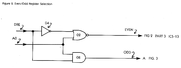
In order to use this new register, we need to expand our addressing
capability. Figure 2 shows a way to use the Address 0 line to select even
and odd addresses in the device register space.
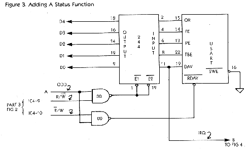
STATUS REGISTER
Figure 3 shows an implementation of the status register. The 74HCT244
shown is a tri-state buffer. This allows us to read the status bits when
we select any odd address in the device register space. The gate to the
USART RDAV pin resets the Data Available flip-flop when we write anything
to an odd address.
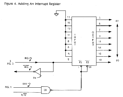
The IRQ line is there in case you want to design in an Interrupt
Register. We're assuming that we want to generate an interrupt when we
get a Data Available signal from the USART.
Figure 4 uses a 74HCT244 to make an interrupt register. This
allows the OS interrupt handler to poll our Parallel Bus device to see
who made an interrupt request. By putting the IRQ signal on the Data 0
line, we have established our USART device as Device 0.
Putting the signal on the Data 1 line would make it Device 1,
Data 3 makes it Device 3, etc. Whatever bit you use here must correspond
to the bit you use for the Enable Latch (Figure 1). The remaining bits
must be tied to 0 (Ground).
Remember that we've designed this circuit to be the only external
device on the parallel bus. If you were to put several devices on the bus,
things would get much more complex. Designing a multiple board system is
beyond the scope of this article.
But if you're a serious hardware hacker, you can probably extend
what we've done here for more than one function. You should also realize
that the logic in this design can be streamlined in several places. We
aimed for use of only a few IC types, and haven't always optimized for
speed or elegance. Sometimes we do things like use a NOR and an inverter
to make an OR gate. Bulky, but workable.
YOUR SOFTWARE
Now for software The only really awkward thing here is that you've
got to have access to an EPROM programmer for 2716's. I used a cranky home-built
programmer a friend put together. Most large users' groups have at least
one member with access to one, so you might try there. The important part
of the ROM is the vector table. You can put all your device driver routines
on disk and load them as an AUTORUN.SYS file if you want, but the vector
table MUST be in ROM. You can also put your device drivers in ROM if you
want.
For our example, we are only implementing INIT, PUT, GET, and
STATUS. For simplicity, we're making the drivers contiguous with the ROM
vector table to run entirely from ROM.
The drivers in Listing 1 were written using MAC/65 (Optimized
Systems Software). The source code will also assemble using the Atari Assembler
Editor cartridge.
The drivers are thoroughly commented so it should be easy for
you to see how they work. Notice that we reset the CRITIC flag at the beginning
of each driver routine. The Generic Handler sets it in advance in case
a parallel device is extremely time critical.
Forgetting to reset CRITIC defeats some OS functions such as
software counter timers and key repeat among others. The rest of the code
is very straightforward. Many thanks to Dave Menconi, formerly of Atari,
for the easy-to-follow listing.
Using these basic ideas with some ingenuity, you should be able
to design your own parallel devices for your 800XL or 600XL computer. If
you dream up an interesting project, the editors at Antic would like to
hear about it.
Earl Rice headed users' group support and was an engineering project leader for Atari.