Anatomy of an 800XL
Inside the belly of the beast
By Robert Dewitt, Managing Editor
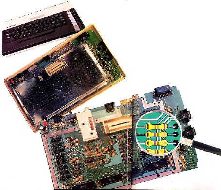
For those of you who are curious about the innards of the XL computers, here is a guided tour of the inside of an Atari 80OXL. We were treated to this tour by the engineering staff at Atari. Please note that there are some differences between the 800 XL and the other XL computers.
It isn't hard to take the computer apart, but if you open the case you void your warranty. Perhaps this article will quench your desire to do so.
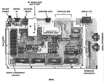 800 XL
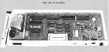 600 XL
The top of the case is attached by screws to the bottom, and is easily removed, but you should be careful with the ribbon connector that plugs the keyboard into the printed-circuit board. This connection is the most delicate in the whole assembly, and frequent detachment of it is not recommended.
The metal plate that covers most of the printed-circuit (PC) board suppresses radio-frequency (RF) interference. The exposed arrays of resistors and condensers at the immediate right of the plate also serve that function. The controller ports are mounted at the extreme right, and the serial 1/0 plug is at the upper right.
Under the RF plate are the other components. Arranged along the front are the major chips. From left to right they are: GTIA, ANTIC, the 6502, and PIA. POKEY is directly above PIA. In the 60OXL, the positions of GTIA and ANTIC are reversed.
The two chips just to the left of the keyboard connector are the keyboard decoders. Above them are the Operating System and BASIC chips. The cartridge slot is obvious. The parallel bus is located just above the cartridge slot at the back of the computer.
Between the cartridge slot and the 6502 are the address-decoder chips, the RAM-timing chips, and several chips that are described as "glue" for the system. There are far fewer glue chips in the XLs than in previous Atari computers.
Immediately above the ANTIC chip is the audio/video analog circuitry that culminates in the rectangular RF modulator box at the back of the machine. To its left is the monitor jack. Note that this jack has only three leads: audio, luminance, and composite video; chroma is not independently available as it was with the Atari 800.
To the right of the RF modulator are the channel switch, the power-in connector, and the ON/OFF switch. Note that the power connector is a DIN plug. It is designed to prevent the accidental connection of a power cord from older Atari computers.
The eight chips that line the left side are "64K by one-bit" RAM chips. In the front left corner is the color-adjustment circuit. Above the GTIA and to the right of the RAM chips are the dynamic-RAM address multiplexors. Further up is the master clock. The intervening gap is reserved for the circuits needed by the XLs prepared for international markets.
When you power-up the 80OXL, the first thing that starts is the clock. The reset stabilizer then initializes certain latches in the PIA, so that the 6502 can find the Operating System, and sets ANTIC to a known state of non-display. Then the 6502 kicks in, and goes to address $FFFC. This vectors it to the initialization routines.